Research
Emerging Device Architectures
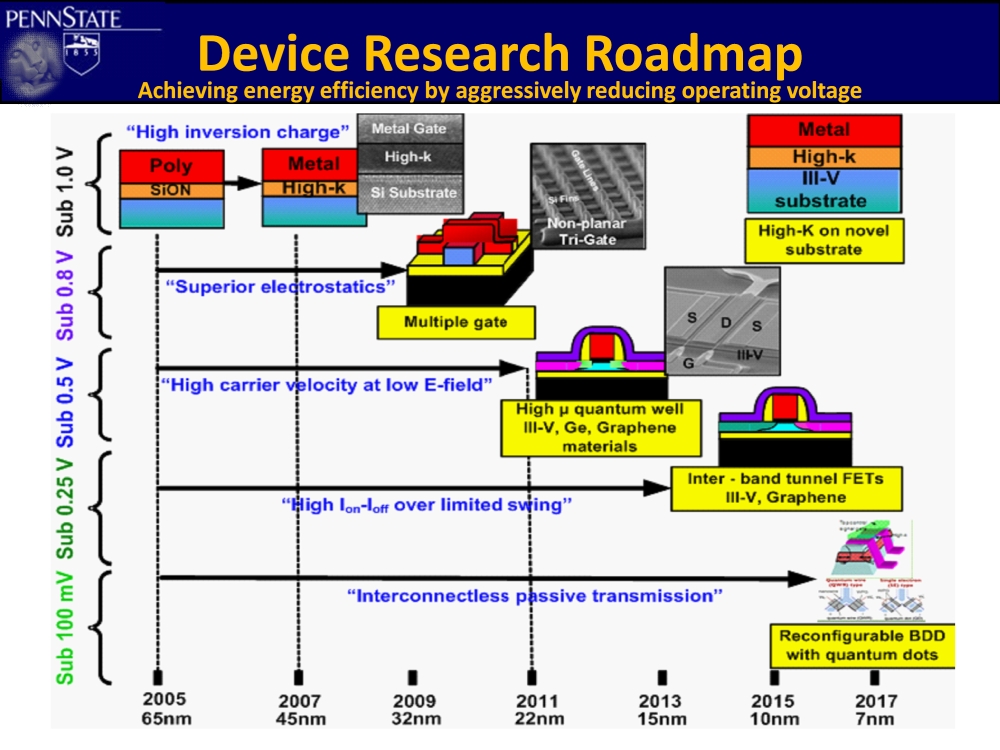
There are several ongoing research projects in our group related to energy efficient nanoelectronics. Broadly, our research efforts are directed at developing novel devices and circuits for more-of-Moore and more-than-Moore applications. In the more-of-Moore effort, we are investigating a gamut of
emerging device architecture incorporating new materials that will enable aggressive operating voltage scaling for energy efficient computing applications. In the more-than-Moore effort, we are investigating multifunctional materials and devices that can integrate novel on-chip sensing functionalities with the state-of-the-art information processing.
Click here to learn more
High-k Dielectric Gated Quantum-Well Transistors
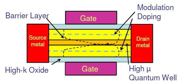
This research involves investigation of an optimal scalable architecture for compound semiconductor based quantum-well transistors (QWFETs) in the narrow gap CS materials space. Arsenic and antimonide based compound semiconductor based materials are under consideration for possible replacement of the silicon channels in future CMOS transistors. We have a tightly coupled research agenda that is investigating the following : a) design and demonstrate a
scalable quantum well transistor architecture which employs self-aligned charge transfer doped source drain extensions, b) demonstration of a
planar architecture instead of recessed gate enabled by high quality gate dielectric incorporation and surface charge compensation, c) demonstration of hole transport enhancement using strain engineering to enable a complementary logic solution d) fabrication of deep sub-micron gate length transistors to extract and benchmark source velocity as a function of gate length, short channel effects for sub 0.5V operating voltage range. This study will provide key insight into the feasibility of CS based narrow gap material such as In
xGa
1-xAs (0.53 < x < 1) and InAs
1-ySb
y (y ≥ 0.2) as a channel material and incubate new ideas to enhance the energy efficiency of complementary logic transistors. This research is funded by the SRC and DARPA under the
Materials, Structures and Devices focus center research center (FCRP)
Click here to learn more
Inter-band Tunnel Transistors and Related Circuits
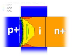
This research is directed at demonstrating the minimum energy-delay product performance of inter-band tunneling transistors that can be realized by using narrow and direct gap high mobility heterostructure materials, such as In
xGa
1-xAs (0.53 < x < 1) . The goal of this research is to create a non-equilibrium distribution of carriers via inter-band tunneling process from degenerately doped source region into the channel with the high/low energy portions of the Fermi-Dirac distribution filtered by the valence/conduction band edges of the source and channel semiconductor, respectively. This can result in sub kT/q steep sub-threshold slope transistors with high Ion-Ioff over a limited gate voltage swing (<0.35V). The key research challenge is to experimentally demonstrate a tunnel transistor with acceptable on-current by enhancing the source-side tunnel injection coefficient. This can be achieved by an optimal combination of narrow/direct gap, low effective mass material system, band-gap engineering using heterostructure, sharp doping profile in conjunction with low temperature processing, phonon engineering, low EOT dielectric integration and finally, multiple gate architecture with efficient gate-to-channel coupling. Our ongoing research addresses several open questions through a combination of theory and experiments: Can abrupt doping profile be maintained throughout fabrication process? Can a high quality ultra-thin high-k dielectric be integrated in a vertical transistor configuration? What is the role of remote and surface phonon scattering on inter-band tunneling properties near material interfaces, and can it be tuned using heterostructure superlattice constructs in III-V material systems? Will non-equilibrium carrier distributions induced by inter-band electron tunneling result in more or less severe dissipative bottlenecks? Our research seeks to optimize both n-channel and p-channel tunnel transistor performance within the framework of a compatible device architecture so that ultra-low power complementary digital electronics can be realized with record energy-delay metric over traditional CMOS. This research is funded by the NRI (Nanoelectronics Research Initiative) and SRC under the
MIND research center
Click here to learn more
Sub Hundred Millivolt Supply Voltage Logic Architecture
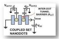
Many emerging nanoscale devices, charge or alternate state variable based, exhibit low transconductance and output resistance under very low operating voltage conditions, making it essential to reconsider device design in conjunction with new logic representation. To circumvent the limited device gain related issues at low voltages, we are exploring a novel interconnectless binary decision diagram (BDD) based logic architecture based on 2 classes of building blocks such as wrapped gate nanowires and split gate nanodots. The proposed architecture produces a) lower device count than conventional Boolean CMOS logic, b) reduces wiring related energy loss, maintains logic functionality under tens of millivolts of supply voltage, and c) operates with ultra-low energy-delay product. All combinational functions can be realized with the nanodot-based BDD approach and sequential logic functions such as latches, shift registers, flipflops can be realized by interfacing with feedback circuits using nanowire transistors. Our ongoing theoretical and experimental research is investigating whether the aggregate can better the projected state of the art for CMOS for the entire range of information processing tasks. This program is supported by a federal government agency.
Click here to learn more
On Chip Magnetoelectric Sensor
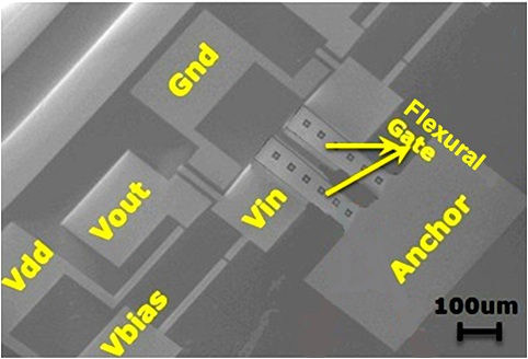
A novel chip-scale ultra-sensitive magnetic sensor, MagnetoElectric Flexural Gate Transistor (MEFGT) capable of measuring pico Tesla biomagnetic field and capable of operating at room temperature has been developed in this research program. To achieve such a high sensitivity, a thin film magnetostrictive material (Metglas
(R)) comprising of high magnetization and low coercivity has been developed with high magnetoelectric coefficient. To further improve the sensitivity, several novel approaches are being pursued such as magnetic flux concentration effect and resonance mode detection. The integrated MEMS device using magnetostrictive cantilever and FET sensing and amplifying capability exhibits a significant enhancement in the signal-to-noise ratio and consequently smaller minimum AC magnetic field detection capability. Also, this demonstration indicates the compatibility of the nanofabricated ME sensors with the Si process technology and provides the feasibility step for implementing ultra sensitive chip-scale magnetometers in highly miniaturized form-factor. Signal readout circuitry with very low input noise and low parasitic effects, fabricated using standard semiconductor processing technology, are being directly integrated with the magnetic sensors. This program is supported by National Science Foundation.
Click here to learn more
Graphene based RF Devices and Circuits
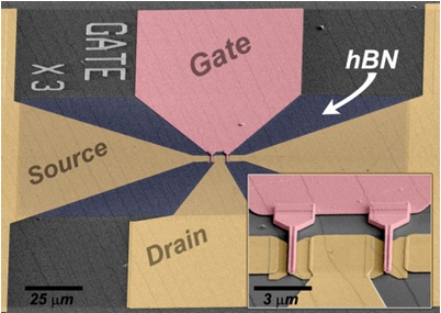
This research focuses on the fabrication and optimization of graphene based devices for practical applications.? Graphene is a recently discovered material that has attracted great interest in recent years for its unique physics, high carrier mobility, symmetric ambipolar behavior, and 2-dimensional planar structure.? It consists of a hexagonal lattice of sp2 hybridized carbon atoms, where the delocalized pi-bonds and unique, linear band structure lead to phenomenal electronic transport properties, with reported mobilities as high as 200,000 cm
2/V sec.? Although graphene devices have made significant progress in a very short period of time, there are several fundamental challenges that must be overcome to develop a practical graphene based technology for digital or analog applications.? Primary among these challenges are 1) the semi-metal nature of graphene (lack of true bandgap), which limits the on-off ratio of graphene devices to the order of 10; 2) development of low contact resistance metal-graphene contact; and 3) control of graphene growth and materials integration in order to preserve the excellent electronic properties of graphene in practical devices.? Our research aims to address these key areas while providing insight into the fundamental limits facing graphene based devices.? Currently, efforts are focused on work function engineering at the metal-graphene interface to optimize device performance and reduce parasitic resistances, reducing access resistance through use of source/drain doping and/or self-aligned processes, and demonstration of optimized, deep sub-micron gate length RF transistors with excellent extrinsic RF performance.
Click here to learn more
Variation in Emering Devices
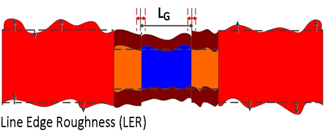
This research compares the variation handling capabilities of Silicon and III-V based novel devices. FINFETs or Tri-Gate transistors have emerged as promising device architecture for 22nm node and beyond logic applications. For sub-10nm node applications, high mobility III-V materials such as In
0.53Ga
0.47As are under investigation to replace the Silicon channel in FINFETs to further enhance performance. Strong quantum confinement effects in In
0.53Ga
0.47As FINFETs make them more sensitive to Fin LER variation than Silicon. However, better electrostatics in In
0.53Ga
0.47As, due to higher effective channel length from lower SD doping, reduces L
G variation impact in In
0.53Ga
0.47As FINFETs that compensates for the increased variation from quantum confinement effect. Tighter control of Fin LER in In
0.53Ga
0.47As together with improved short channel immunity will make III-VFINFETs a promising device for 0.5V and below logic applications. This program is supported by Lam Research Corporation.
Click here to learn more
Ballistic Deflection Devices
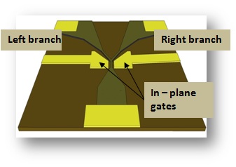
This research project involves the investigation of ballistic electron transport properties in high ¨C mobility III-V semiconductors and further looks at how to exploit these effects to realize ultra ¨C low power logic devices. Emerging nanoscale devices, charge or alternate state variable based, exhibit very low intrinsic gain at reduced operating voltage conditions, making it essential to reconsider device design in conjunction with new logic representation. In this project we are exploring a novel interconnect-less binary decision diagram (BDD) logic architecture based on ballistic propagation of electrons in the so called Y-junction switch. The proposed architecture a) circumvents the need to charge and discharge load capacitances at each node in the logic tree thus dramatically reducing propagation delay, b)reduces wiring related energy loss while maintaining logic functionality under tens of millivolts of supply voltage, and c) operates with ultra-low energy-delay product. BDD architecture lends itself well towards design with ballistic Y-junction and nanowire devices. Our ongoing theoretical and experimental research is investigating whether this approach is indeed suitable for augmenting/replacing CMOS logic at ultra ¨C low supply voltages. This program is supported by a federal government agency.
Click here to learn more
Soft Error in Emerging Devices
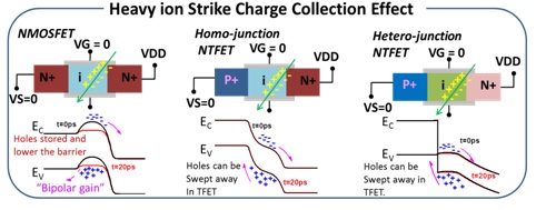
This research project focuses on radiation induced single-event upset (SEU) in emerging devices. Soft error has become a key challenge for cloud computing with growing number of processors in data center. With proposed introduction of low bandgap materials (Ge, III-Vs) as channel replacement and steep switching devices for low voltage application, charge generation from sea-level neutron radiation needs to be evaluated due to their low ionization energy. In this project, the soft error generation and propagation in Si FinFET, III-V FinFET and III-V Hetero-junction Tunnel FET (HTFET) are investigated using device and circuit simulation. The device simulation shows that III-V FinFET presents enhanced charge collection, while HTFET presents significant reduction of the bipolar gain effect and charge collection. Based on the critical LET extraction, SRAM bit-flip, electrical masking effect as well as the latching window masking effect has been analyzed for these devices. The SER performance evaluation of SRAM and Logic with voltage scaling shows that HTFET based SRAM and Logic are desirable for radiation resilient ultra-low power application. III-V FinFET shows increased charge deposition due to low ionization energy, which increases the SER for SRAM cell for all V
DD compared to Si FinFET. For Logic, III-V FinFET shows reduced SER than Si FinFET below 0.5V.
Click here to learn more

 There are several ongoing research projects in our group related to energy efficient nanoelectronics. Broadly, our research efforts are directed at developing novel devices and circuits for more-of-Moore and more-than-Moore applications. In the more-of-Moore effort, we are investigating a gamut of emerging device architecture incorporating new materials that will enable aggressive operating voltage scaling for energy efficient computing applications. In the more-than-Moore effort, we are investigating multifunctional materials and devices that can integrate novel on-chip sensing functionalities with the state-of-the-art information processing.
 This research involves investigation of an optimal scalable architecture for compound semiconductor based quantum-well transistors (QWFETs) in the narrow gap CS materials space. Arsenic and antimonide based compound semiconductor based materials are under consideration for possible replacement of the silicon channels in future CMOS transistors. We have a tightly coupled research agenda that is investigating the following : a) design and demonstrate a scalable quantum well transistor architecture which employs self-aligned charge transfer doped source drain extensions, b) demonstration of a planar architecture instead of recessed gate enabled by high quality gate dielectric incorporation and surface charge compensation, c) demonstration of hole transport enhancement using strain engineering to enable a complementary logic solution d) fabrication of deep sub-micron gate length transistors to extract and benchmark source velocity as a function of gate length, short channel effects for sub 0.5V operating voltage range. This study will provide key insight into the feasibility of CS based narrow gap material such as InxGa1-xAs (0.53 < x < 1) and InAs1-ySby (y ≥ 0.2) as a channel material and incubate new ideas to enhance the energy efficiency of complementary logic transistors. This research is funded by the SRC and DARPA under the Materials, Structures and Devices focus center research center (FCRP)
 This research is directed at demonstrating the minimum energy-delay product performance of inter-band tunneling transistors that can be realized by using narrow and direct gap high mobility heterostructure materials, such as InxGa1-xAs (0.53 < x < 1) . The goal of this research is to create a non-equilibrium distribution of carriers via inter-band tunneling process from degenerately doped source region into the channel with the high/low energy portions of the Fermi-Dirac distribution filtered by the valence/conduction band edges of the source and channel semiconductor, respectively. This can result in sub kT/q steep sub-threshold slope transistors with high Ion-Ioff over a limited gate voltage swing (<0.35V). The key research challenge is to experimentally demonstrate a tunnel transistor with acceptable on-current by enhancing the source-side tunnel injection coefficient. This can be achieved by an optimal combination of narrow/direct gap, low effective mass material system, band-gap engineering using heterostructure, sharp doping profile in conjunction with low temperature processing, phonon engineering, low EOT dielectric integration and finally, multiple gate architecture with efficient gate-to-channel coupling. Our ongoing research addresses several open questions through a combination of theory and experiments: Can abrupt doping profile be maintained throughout fabrication process? Can a high quality ultra-thin high-k dielectric be integrated in a vertical transistor configuration? What is the role of remote and surface phonon scattering on inter-band tunneling properties near material interfaces, and can it be tuned using heterostructure superlattice constructs in III-V material systems? Will non-equilibrium carrier distributions induced by inter-band electron tunneling result in more or less severe dissipative bottlenecks? Our research seeks to optimize both n-channel and p-channel tunnel transistor performance within the framework of a compatible device architecture so that ultra-low power complementary digital electronics can be realized with record energy-delay metric over traditional CMOS. This research is funded by the NRI (Nanoelectronics Research Initiative) and SRC under the MIND research center
 Many emerging nanoscale devices, charge or alternate state variable based, exhibit low transconductance and output resistance under very low operating voltage conditions, making it essential to reconsider device design in conjunction with new logic representation. To circumvent the limited device gain related issues at low voltages, we are exploring a novel interconnectless binary decision diagram (BDD) based logic architecture based on 2 classes of building blocks such as wrapped gate nanowires and split gate nanodots. The proposed architecture produces a) lower device count than conventional Boolean CMOS logic, b) reduces wiring related energy loss, maintains logic functionality under tens of millivolts of supply voltage, and c) operates with ultra-low energy-delay product. All combinational functions can be realized with the nanodot-based BDD approach and sequential logic functions such as latches, shift registers, flipflops can be realized by interfacing with feedback circuits using nanowire transistors. Our ongoing theoretical and experimental research is investigating whether the aggregate can better the projected state of the art for CMOS for the entire range of information processing tasks. This program is supported by a federal government agency.
 A novel chip-scale ultra-sensitive magnetic sensor, MagnetoElectric Flexural Gate Transistor (MEFGT) capable of measuring pico Tesla biomagnetic field and capable of operating at room temperature has been developed in this research program. To achieve such a high sensitivity, a thin film magnetostrictive material (Metglas(R)) comprising of high magnetization and low coercivity has been developed with high magnetoelectric coefficient. To further improve the sensitivity, several novel approaches are being pursued such as magnetic flux concentration effect and resonance mode detection. The integrated MEMS device using magnetostrictive cantilever and FET sensing and amplifying capability exhibits a significant enhancement in the signal-to-noise ratio and consequently smaller minimum AC magnetic field detection capability. Also, this demonstration indicates the compatibility of the nanofabricated ME sensors with the Si process technology and provides the feasibility step for implementing ultra sensitive chip-scale magnetometers in highly miniaturized form-factor. Signal readout circuitry with very low input noise and low parasitic effects, fabricated using standard semiconductor processing technology, are being directly integrated with the magnetic sensors. This program is supported by National Science Foundation.
 This research focuses on the fabrication and optimization of graphene based devices for practical applications.? Graphene is a recently discovered material that has attracted great interest in recent years for its unique physics, high carrier mobility, symmetric ambipolar behavior, and 2-dimensional planar structure.? It consists of a hexagonal lattice of sp2 hybridized carbon atoms, where the delocalized pi-bonds and unique, linear band structure lead to phenomenal electronic transport properties, with reported mobilities as high as 200,000 cm2/V sec.? Although graphene devices have made significant progress in a very short period of time, there are several fundamental challenges that must be overcome to develop a practical graphene based technology for digital or analog applications.? Primary among these challenges are 1) the semi-metal nature of graphene (lack of true bandgap), which limits the on-off ratio of graphene devices to the order of 10; 2) development of low contact resistance metal-graphene contact; and 3) control of graphene growth and materials integration in order to preserve the excellent electronic properties of graphene in practical devices.? Our research aims to address these key areas while providing insight into the fundamental limits facing graphene based devices.? Currently, efforts are focused on work function engineering at the metal-graphene interface to optimize device performance and reduce parasitic resistances, reducing access resistance through use of source/drain doping and/or self-aligned processes, and demonstration of optimized, deep sub-micron gate length RF transistors with excellent extrinsic RF performance.
 This research compares the variation handling capabilities of Silicon and III-V based novel devices. FINFETs or Tri-Gate transistors have emerged as promising device architecture for 22nm node and beyond logic applications. For sub-10nm node applications, high mobility III-V materials such as In0.53Ga0.47As are under investigation to replace the Silicon channel in FINFETs to further enhance performance. Strong quantum confinement effects in In0.53Ga0.47As FINFETs make them more sensitive to Fin LER variation than Silicon. However, better electrostatics in In0.53Ga0.47As, due to higher effective channel length from lower SD doping, reduces LG variation impact in In0.53Ga0.47As FINFETs that compensates for the increased variation from quantum confinement effect. Tighter control of Fin LER in In0.53Ga0.47As together with improved short channel immunity will make III-VFINFETs a promising device for 0.5V and below logic applications. This program is supported by Lam Research Corporation.
 This research project involves the investigation of ballistic electron transport properties in high ¨C mobility III-V semiconductors and further looks at how to exploit these effects to realize ultra ¨C low power logic devices. Emerging nanoscale devices, charge or alternate state variable based, exhibit very low intrinsic gain at reduced operating voltage conditions, making it essential to reconsider device design in conjunction with new logic representation. In this project we are exploring a novel interconnect-less binary decision diagram (BDD) logic architecture based on ballistic propagation of electrons in the so called Y-junction switch. The proposed architecture a) circumvents the need to charge and discharge load capacitances at each node in the logic tree thus dramatically reducing propagation delay, b)reduces wiring related energy loss while maintaining logic functionality under tens of millivolts of supply voltage, and c) operates with ultra-low energy-delay product. BDD architecture lends itself well towards design with ballistic Y-junction and nanowire devices. Our ongoing theoretical and experimental research is investigating whether this approach is indeed suitable for augmenting/replacing CMOS logic at ultra ¨C low supply voltages. This program is supported by a federal government agency.
 This research project focuses on radiation induced single-event upset (SEU) in emerging devices. Soft error has become a key challenge for cloud computing with growing number of processors in data center. With proposed introduction of low bandgap materials (Ge, III-Vs) as channel replacement and steep switching devices for low voltage application, charge generation from sea-level neutron radiation needs to be evaluated due to their low ionization energy. In this project, the soft error generation and propagation in Si FinFET, III-V FinFET and III-V Hetero-junction Tunnel FET (HTFET) are investigated using device and circuit simulation. The device simulation shows that III-V FinFET presents enhanced charge collection, while HTFET presents significant reduction of the bipolar gain effect and charge collection. Based on the critical LET extraction, SRAM bit-flip, electrical masking effect as well as the latching window masking effect has been analyzed for these devices. The SER performance evaluation of SRAM and Logic with voltage scaling shows that HTFET based SRAM and Logic are desirable for radiation resilient ultra-low power application. III-V FinFET shows increased charge deposition due to low ionization energy, which increases the SER for SRAM cell for all VDD compared to Si FinFET. For Logic, III-V FinFET shows reduced SER than Si FinFET below 0.5V.
